October 2023
As smaller, cheaper, more powerful microchips continue to transform the global economy, a little-known company in the Netherlands has emerged as a vital linchpin in the semiconductor industry. Here, Walter Scott investment manager Tom Miedema writes about ASML and its groundbreaking EUV lithography machines.
Highlights
- ASML is a leading player in lithography machines – equipment used to produce microchips
- Some of ASML’s machines cost up to US$200 million apiece1
- By 2029, the value of the global semiconductor market is projected to reach US$1,381 billion2
A Dutch commuter town might not be the first place you would expect to find a company operating at the frontier of technology and innovation, but Veldhoven, some 15 minutes southeast of Eindhoven, is home to a company often dubbed “the most important tech company you’ve never heard of.” For once, such a lofty claim is not hyperbole: ASML (Advanced Semiconductor Materials Lithography) is certainly no household name, but without its groundbreaking work much of the technology we take for granted today would not be possible.
Since its founding in 1984, ASML has been integral to the semiconductor ecosystem and a key enabler of Moore’s Law, the empirical observation made by Gordon Moore, the co-founder of Intel, that states that the number of transistors in a given area of a semiconductor will double every two years, exponentially increasing the computing power while decreasing the cost of the chip. The resultant smaller, cheaper, more powerful chips are the keystones of our current technology revolution, transforming every corner of the global economy, from communication and entertainment to healthcare and industrial manufacturing.
What is EUV lithography?
Spun out of Dutch electronics giant Philips in 1995, ASML has grown to become the leading player in one of the critical steps in the production of semiconductors – lithography. The process of using light to trace integrated circuits onto silicon wafers, it is lithography that determines how small the features on a chip can be, and how densely manufacturers can pack transistors together. Progress in lithography is predicated on ever shorter light wavelengths – the shorter the wavelength, the smaller the features that can be printed in a lithography process. Today, the most advanced form of lithography technology is EUV. Occurring naturally in outer space, EUV light has a wavelength 14 times shorter than deep ultraviolet (DUV) light, the previously most advanced technology used in lithography. The result of huge investment and decades of research and development (R&D), EUV lithography has been credited with “saving” Moore’s Law and ensuring it may extend well into this next decade and potentially beyond.
Little competition for ASML
To date, only one company in the world has mastered EUV lithography: ASML3. Long the leading player in DUV with a market share that dwarf those of its two main competitors Nikon and Canon, for more than two decades the company has worked to develop a commercially viable EUV system. The importance of the prospective technology to the semiconductor industry was evidenced in 2012 by large-scale investment in the development process from TSMC, Samsung and Intel. To accelerate the development of key technologies, ASML launched a series of astute acquisitions, including Cymer (lithography light sources) in 2012 and Hermes Microvision (e-beam metrology) in 2016, while at the same time working collaboratively with two German companies, Zeiss and Trumpf, to develop the necessary optical instruments and lasers. Finally, having overcome considerable scientific and technological challenges, ASML launched the TWINSCAN NXE:3400, a system that one technology insider has labelled “the most complicated machine humans have built.”
Even a cursory explanation of what occurs inside these machines gives a sense of the complexity involved. Every second, 50,000 droplets of molten tin are hit by two lasers. The first laser flattens the droplet, while the second vaporizes it to create a plasma that projects light onto a blueprint of the pattern that will be printed on the chip via a highly complex system of exceptionally precise mirrors (the mirrors are so smooth that if expanded to the size of Germany they would not have a bump higher than a millimeter). The pattern, now encoded in the light, is then printed onto a silicon wafer. Pattern is laid upon pattern hundreds of times over before the semiconductor is complete. Comprising more than 100,000 components, each machine will cost the purchaser up to US$200 million – complexity on this scale does not come cheap.
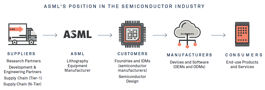
It is through this combination of technical proficiency, vertical integration, and collaboration, that ASML has established its de facto ownership of the EUV lithography equipment machine market, which, given the high barriers to entry created by its technical complexity and the requirement for large-scale investment, is unlikely to face challenge for the foreseeable future. While demand is still at an early stage (most semiconductors continue to be manufactured using DUV technology), it is now well established and growing fast.
What’s next
We believe demand should continue to grow. A significant portion of the huge capital expenditure plans of Samsung, TSMC and Intel may be directed towards upping their EUV capacity.
Driving this demand is one of the global economy’s most compelling long-term growth trends: the expansion of the world’s digital infrastructure and the increasing prevalence of semiconductors across sectors. By 2029, the value of the global semiconductor market is projected to reach US$1,381 billion, up from US$573 billion in 2022, a compound annual growth rate of 12.2%3. Few, if any, industries are untouched by the digital revolution, and the emerging trends of recent years, artificial Intelligence, automation, 5G, Big Data and the Internet of Things, have an insatiable appetite for faster and more powerful chips.
1 Reuters. Chipmaker ASML raises full-year sales forecast as China demand stays strong. July 2023.
2 Fortune Business Insights. April 2022.
3 IBM. Why we need EUV lithography for the future of chips. June 2023.
All investments involve risk, including the possible loss of principal. Certain investments involve greater or unique risks that should be considered along with the objectives, fees, and expenses before investing. Company information is mentioned only for informational purposes and should not be construed as investment or any other advice. The holdings listed should not be considered recommendations to buy or sell a security.
BNY Mellon Investment Management is one of the world’s leading investment management organizations, encompassing BNY Mellon’s affiliated investment management firms and global distribution companies. BNY Mellon is the corporate brand of The Bank of New York Mellon Corporation and may also be used as a generic term to reference the corporation as a whole or its various subsidiaries generally.
This material has been provided for informational purposes only and should not be construed as investment advice or a recommendation of any particular investment product, strategy, investment manager or account arrangement, and should not serve as a primary basis for investment decisions.
Prospective investors should consult a legal, tax or financial professional in order to determine whether any investment product, strategy or service is appropriate for their particular circumstances. Views expressed are those of the author stated and do not reflect views of other managers or the firm overall. Views are current as of the date of this publication and subject to change.
The information is based on current market conditions, which will fluctuate and may be superseded by subsequent market events or for other reasons. References to specific securities, asset classes and financial markets are for illustrative purposes only and are not intended to be and should not be interpreted as recommendations. Information contained herein has been obtained from sources believed to be reliable, but not guaranteed. No part of this material may be reproduced in any form, or referred to in any other publication, without express written permission.
Walter Scott & Partners Limited (“Walter Scott”) is an investment management firm authorized and regulated in the United Kingdom by the Financial Conduct Authority in the conduct of investment business. Walter Scott is also registered with the U.S. Securities and Exchange Commission (SEC) as an investment adviser. Walter Scott is a subsidiary of The Bank of New York Mellon Corporation.
Not FDIC-Insured | No Bank Guarantee | May Lose Value
© 2023 BNY Mellon Securities Corporation, distributor, 240 Greenwich Street, 9th Floor, New York, NY 10286
MARK-429508-2023-09-26